| Parameter
|
0.15um
|
0.4um
|
0.25um
|
| Imax (mA/mm)
|
1150
|
1190
|
1200
|
| Idss(mA/mm)
|
910
|
730
|
750
|
| Gm (mS/mm)
|
343
|
300
|
330
|
| Vp (V)
|
-3
|
-2.6
|
-2.4
|
| BVgd (V)
|
80
|
>200
|
>150
|
| MAG @ 2.0 GHz (dB)
|
16
|
>24
|
>26
|
| ƒT(GHz)
|
42
|
19
|
23
|
| ƒmax(GHz)
|
170
|
62
|
100
|
| Pout (W/mm)@3.5 GHz,Vds-48V
|
N/A
|
13.5
|
11.0
|
| PAE(%)@3.5GHz, Vds-48V
|
N/A
|
81.0
|
79
|
| Pout (W/mm)@15 GHz,Vds-28V
|
N/A
|
N/A
|
4.0
|
| PAE(%)@15GHz, Vds-28V
|
N/A
|
N/A
|
45
|
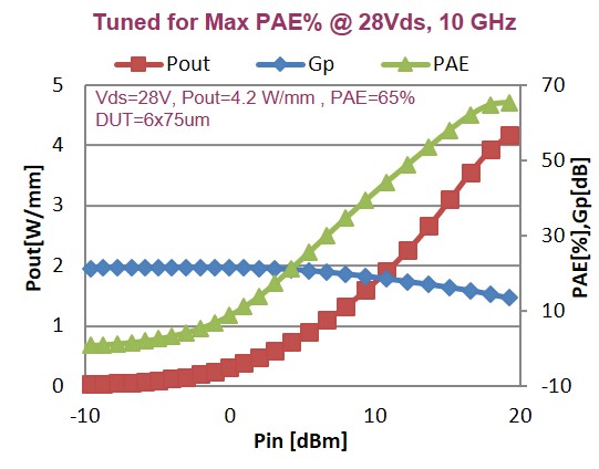
| Pout (W/mm)@10 GHz,Vds-48V
|
N/A
|
10.3
|
10.8
|
| Max. Drain Eff. (%) @10 GHz,Vds-48V
|
N/A
|
57
|
65
|
| Nfmin@10 GHz -28V
|
N/A
|
1.15dB
|
1.1dB
|
| MXP Psat (W/mm) @ 18GHz, Vds = 28V
|
5
|
N/A
|
N/A
|
| MXE PAE (%) @ 18GHz, Vds = 28V
|
60
|
N/A
|
N/A
|
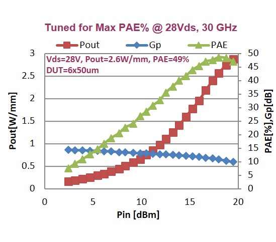
| MXP Psat (W/mm) @ 30GHz, Vds = 28V
|
4.6
|
N/A
|
N/A
|
| MXE PAE (%) @ 30GHz, Vds = 28V
|
49
|
N/A
|
N/A
|
| NFmin (dB) @ 18GHz, Vds = 20V
|
0.77
|
N/A
|
N/A
|
| *Measured at 2 GHz
|